3D revolution and tissue repair
Curator: Larry H. Bernstein, MD, FCAP
Berkeley Lab captures first high-res 3D images of DNA segments

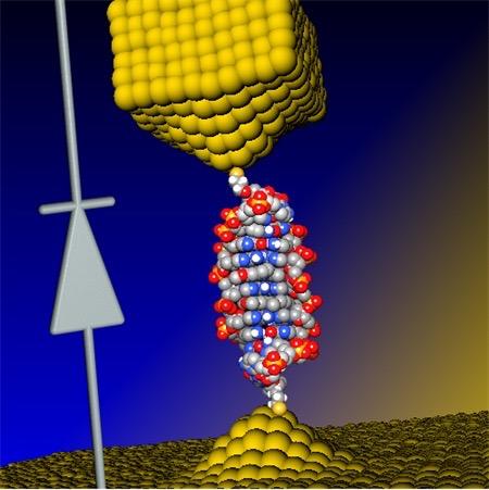
In a Berkeley Lab-led study, flexible double-helix DNA segments (purple, with green DNA models) connected to gold nanoparticles (yellow) are revealed from the 3D density maps reconstructed from individual samples using a Berkeley Lab-developed technique called individual-particle electron tomography (IPET). Projections of the structures are shown in the green background grid. (credit: Berkeley Lab)
An international research team working at the Lawrence Berkeley National Laboratory (Berkeley Lab) has captured the first high-resolution 3D images of double-helix DNA segments attached at either end to gold nanoparticles — which could act as building blocks for molecular computer memory and electronic devices (see World’s smallest electronic diode made from single DNA molecule), nanoscale drug-delivery systems, and as markers for biological research and for imaging disease-relevant proteins.
The researchers connected coiled DNA strands between polygon-shaped gold nanoparticles and then reconstructed 3D images, using a cutting-edge electron microscope technique coupled with a protein-staining process and sophisticated software that provided structural details at the scale of about 2 nanometers.
“We had no idea about what the double-strand DNA would look like between the gold nanoparticles,” said Gang “Gary” Ren, a Berkeley Lab scientist who led the research. “This is the first time for directly visualizing an individual double-strand DNA segment in 3D,” he said.
The results were published in an open-access paper in the March 30 edition of Nature Communications.
The method developed by this team, called individual-particle electron tomography (IPET), had earlier captured the 3-D structure of a single protein that plays a key role in human cholesterol metabolism. By grabbing 2D images of an object from different angles, the technique allows researchers to assemble a 3D image of that object.
The team has also used the technique to uncover the fluctuation of another well-known flexible protein, human immunoglobulin 1, which plays a role in the human immune system.
https://youtu.be/lQrbmg9ry90
Berkeley Lab | 3-D Reconstructions of Double strand DNA and Gold Nanoparticle Structures
For this new study of DNA nanostructures, Ren used an electron-beam study technique called cryo-electron microscopy (cryo-EM) to examine frozen DNA-nanogold samples, and used IPET to reconstruct 3-D images from samples stained with heavy metal salts. The team also used molecular simulation tools to test the natural shape variations (“conformations”) in the samples, and compared these simulated shapes with observations.
First visualization of DNA strand dynamics without distorting x-ray crystallography
Ren explained that the naturally flexible dynamics of samples, like a man waving his arms, cannot be fully detailed by any method that uses an average of many observations.
A popular way to view the nanoscale structural details of delicate biological samples is to form them into crystals and zap them with X-rays, but that destroys their natural shape, especially fir the DNA-nanogold samples in this study, which the scientists say are incredibly challenging to crystallize. Other common research techniques may require a collection of thousands of near-identical objects, viewed with an electron microscope, to compile a single, averaged 3-D structure. But an averaged 3D image may not adequately show the natural shape fluctuations of a given object.
The samples in the latest experiment were formed from individual polygon gold nanostructures, measuring about 5 nanometers across, connected to single DNA-segment strands with 84 base pairs. Base pairs are basic chemical building blocks that give DNA its structure. Each individual DNA segment and gold nanoparticle naturally zipped together with a partner to form the double-stranded DNA segment with a gold particle at either end.
https://youtu.be/RDOpgj62PLU
Berkeley Lab | These views compare the various shape fluctuations obtained from different samples of the same type of double-helix DNA segment (DNA renderings in green, 3D reconstructions in purple) connected to gold nanoparticles (yellow).
The samples were flash-frozen to preserve their structure for study with cryo-EM imaging. The distance between the two gold nanoparticles in individual samples varied from 20 to 30 nanometers, based on different shapes observed in the DNA segments.
Researchers used a cryo-electron microscope at Berkeley Lab’s Molecular Foundry for this study. They collected a series of tilted images of the stained objects, and reconstructed 14 electron-density maps that detailed the structure of individual samples using the IPET technique.
Sub-nanometer images next
Ren said that the next step will be to work to improve the resolution to the sub-nanometer scale.
“Even in this current state we begin to see 3-D structures at 1- to 2-nanometer resolution,” he said. “Through better instrumentation and improved computational algorithms, it would be promising to push the resolution to that visualizing a single DNA helix within an individual protein.”
In future studies, researchers could attempt to improve the imaging resolution for complex structures that incorporate more DNA segments as a sort of “DNA origami,” Ren said. Researchers hope to build and better characterize nanoscale molecular devices using DNA segments that can, for example, store and deliver drugs to targeted areas in the body.
“DNA is easy to program, synthesize and replicate, so it can be used as a special material to quickly self-assemble into nanostructures and to guide the operation of molecular-scale devices,” he said. “Our current study is just a proof of concept for imaging these kinds of molecular devices’ structures.”
The team included researchers at UC Berkeley, the Kavli Energy NanoSciences Institute at Berkeley Lab and UC Berkeley, and Xi’an Jiaotong University in China. This work was supported by the National Science Foundation, DOE Office of Basic Energy Sciences, National Institutes of Health, the National Natural Science Foundation of China, Xi’an Jiaotong University in China, and the Ministry of Science and Technology in China. View more about Gary Ren’s research group here.
Abstract of Three-dimensional structural dynamics and fluctuations of DNA-nanogold conjugates by individual-particle electron tomography
DNA base pairing has been used for many years to direct the arrangement of inorganic nanocrystals into small groupings and arrays with tailored optical and electrical properties. The control of DNA-mediated assembly depends crucially on a better understanding of three-dimensional structure of DNA-nanocrystal-hybridized building blocks. Existing techniques do not allow for structural determination of these flexible and heterogeneous samples. Here we report cryo-electron microscopy and negative-staining electron tomography approaches to image, and three-dimensionally reconstruct a single DNA-nanogold conjugate, an 84-bp double-stranded DNA with two 5-nm nanogold particles for potential substrates in plasmon-coupling experiments. By individual-particle electron tomography reconstruction, we obtain 14 density maps at ~2-nm resolution. Using these maps as constraints, we derive 14 conformations of dsDNA by molecular dynamics simulations. The conformational variation is consistent with that from liquid solution, suggesting that individual-particle electron tomography could be an expected approach to study DNA-assembling and flexible protein structure and dynamics.
World’s smallest electronic diode made from single DNA molecule
http://www.kurzweilai.net/worlds-smallest-electronic-diode-made-from-single-dna-molecule

Nanoscale electronic components can be made from single DNA molecules, as researchers at the University of Georgia and at Ben-Gurion University in Israel have demonstrated, using a single molecule of DNA to create the world’s smallest diode.

DNA double helix with base pairs (credit: National Human Genome Research Institute)
A diode is a component vital to electronic devices that allows current to flow in one direction but prevents its flow in the other direction. The development could help stimulate development of DNA components for molecular electronics.
As noted in an open-access Nature Chemistry paper published this week, the researchers designed a 11-base-pair (bp) DNA molecule and inserted a small molecule named coralyne into the DNA.*
They found, surprisingly, that this caused the current flowing through the DNA to be 15 times stronger for negative voltages than for positive voltages, a necessary feature of a diode.
Electronic elements 1,00o times smaller than current components
“Our discovery can lead to progress in the design and construction of nanoscale electronic elements that are at least 1,000 times smaller than current components,” says the study’s lead author, Bingqian Xu an associate professor in the UGA College of Engineering and an adjunct professor in chemistry and physics.
The research team plans to enhance the performance of the molecular diode and construct additional molecular devices, which may include a transistor (similar to a two-layer diode, but with one additional layer).
A theoretical model developed by Yanantan Dubi of Ben-Gurion University indicated the diode-like behavior of DNA originates from the bias voltage-induced breaking of spatial symmetry inside the DNA molecule after the coralyne is inserted.
The research is supported by the National Science Foundation.
*“We prepared the DNA–coralyne complex by specifically intercalating two coralyne molecules into a custom-designed 11-base-pair (bp) DNA molecule (5′-CGCGAAACGCG-3′) containing three mismatched A–A base pairs at the centre,” according to the authors.
UPDATE April 6, 2016 to clarify the coralyne intercalation (insertion) into the DNA molecule.
Abstract of Molecular rectifier composed of DNA with high rectification ratio enabled by intercalation
The predictability, diversity and programmability of DNA make it a leading candidate for the design of functional electronic devices that use single molecules, yet its electron transport properties have not been fully elucidated. This is primarily because of a poor understanding of how the structure of DNA determines its electron transport. Here, we demonstrate a DNA-based molecular rectifier constructed by site-specific intercalation of small molecules (coralyne) into a custom-designed 11-base-pair DNA duplex. Measured current–voltage curves of the DNA–coralyne molecular junction show unexpectedly large rectification with a rectification ratio of about 15 at 1.1 V, a counter-intuitive finding considering the seemingly symmetrical molecular structure of the junction. A non-equilibrium Green’s function-based model—parameterized by density functional theory calculations—revealed that the coralyne-induced spatial asymmetry in the electron state distribution caused the observed rectification. This inherent asymmetry leads to changes in the coupling of the molecular HOMO−1 level to the electrodes when an external voltage is applied, resulting in an asymmetric change in transmission.
references:
- Cunlan Guo, Kun Wang, Elinor Zerah-Harush, Joseph Hamill, Bin Wang, Yonatan Dubi, Bingqian Xu. Molecular rectifier composed of DNA with high rectification ratio enabled by intercalation. Nature Chemistry, 2016; DOI: 10.1038/nchem.2480
- Cunlan Guo, Kun Wang, Elinor Zerah-Harush, Joseph Hamill, Bin Wang, Yonatan Dubi, Bingqian Xu. Molecular rectifier composed of DNA with high rectification ratio enabled by intercalation. Nature Chemistry, 2016; Supplementary Information (open access)
A stem-cell repair system that can regenerate any kind of human tissue …including disease and aging; human trials next year
http://www.kurzweilai.net/a-stem-cell-repair-system-that-can-regenerate-any-kind-of-human-tissue

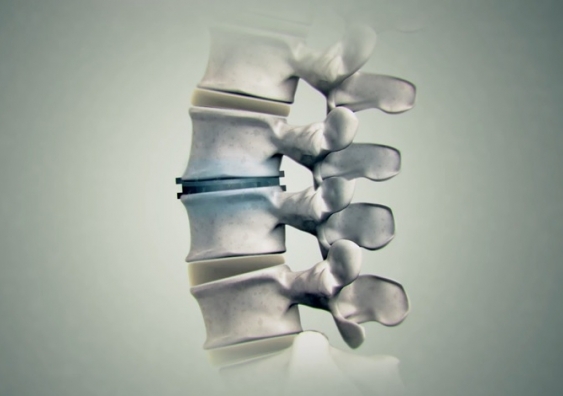
http://www.kurzweilai.net/images/spinal_disc_regeneration.jpg
UNSW researchers say the therapy has enormous potential for treating spinal disc injury and joint and muscle degeneration and could also speed up recovery following complex surgeries where bones and joints need to integrate with the body (credit: UNSW TV)
A stem cell therapy system capable of regenerating any human tissue damaged by injury, disease, or aging could be available within a few years, say University of New South Wales (UNSW Australia) researchers.
Their new repair system*, similar to the method used by salamanders to regenerate limbs, could be used to repair everything from spinal discs to bone fractures, and could transform current treatment approaches to regenerative medicine.
The UNSW-led research was published this week in the Proceedings of the National Academy of Sciences journal.
Reprogramming bone and fat cells
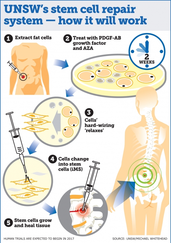
The system reprograms bone and fat cells into induced multipotent stem cells (iMS), which can regenerate multiple tissue types and has been successfully demonstrated in mice, according to study lead author, haematologist, and UNSW Associate Professor John Pimanda.
“This technique is a significant advance on many of the current unproven stem cell therapies, which have shown little or no objective evidence they contribute directly to new tissue formation,” Pimanda said. “We have taken bone and fat cells, switched off their memory and converted them into stem cells so they can repair different cell types once they are put back inside the body.”
“We are currently assessing whether adult human fat cells reprogrammed into iMS cells can safely repair damaged tissue in mice, with human trials expected to begin in late 2017.”
http://www.kurzweilai.net/images/UNSW-stem-cell-repair.jpg
Advantages over stem-cell types
There are different types of stem cells including embryonic stem (ES) cells, which during embryonic development generate every type of cell in the human body, and adult stem cells, which are tissue-specific, but don’t regenerate multiple tissue types. Embryonic stem cells cannot be used to treat damaged tissues because of their tumor forming capacity. The other problem when generating stem cells is the requirement to use viruses to transform cells into stem cells, which is clinically unacceptable, the researchers note.
Research shows that up to 20% of spinal implants either don’t heal or there is delayed healing. The rates are higher for smokers, older people and patients with diseases such diabetes or kidney disease.
Human trials are planned next year once the safety and effectiveness of the technique using human cells in mice has been demonstrated.
* The technique involves extracting adult human fat cells and treating them with the compound 5-Azacytidine (AZA), along with platelet-derived growth factor-AB (PDGF-AB) for about two days. The cells are then treated with the growth factor alone for a further two-three weeks.
AZA is known to induce cell plasticity, which is crucial for reprogramming cells. The AZA compound relaxes the hard-wiring of the cell, which is expanded by the growth factor, transforming the bone and fat cells into iMS cells. When the stem cells are inserted into the damaged tissue site, they multiply, promoting growth and healing.
The new technique is similar to salamander limb regeneration, which is also dependent on the plasticity of differentiated cells, which can repair multiple tissue types, depending on which body part needs replacing.
Along with confirming that human adult fat cells reprogrammed into iMS stem cells can safely repair damaged tissue in mice, the researchers said further work is required to establish whether iMS cells remain dormant at the sites of transplantation and retain their capacity to proliferate on demand.
Abstract of PDGF-AB and 5-Azacytidine induce conversion of somatic cells into tissue-regenerative multipotent stem cells
Current approaches in tissue engineering are geared toward generating tissue-specific stem cells. Given the complexity and heterogeneity of tissues, this approach has its limitations. An alternate approach is to induce terminally differentiated cells to dedifferentiate into multipotent proliferative cells with the capacity to regenerate all components of a damaged tissue, a phenomenon used by salamanders to regenerate limbs. 5-Azacytidine (AZA) is a nucleoside analog that is used to treat preleukemic and leukemic blood disorders. AZA is also known to induce cell plasticity. We hypothesized that AZA-induced cell plasticity occurs via a transient multipotent cell state and that concomitant exposure to a receptive growth factor might result in the expansion of a plastic and proliferative population of cells. To this end, we treated lineage-committed cells with AZA and screened a number of different growth factors with known activity in mesenchyme-derived tissues. Here, we report that transient treatment with AZA in combination with platelet-derived growth factor–AB converts primary somatic cells into tissue-regenerative multipotent stem (iMS) cells. iMS cells possess a distinct transcriptome, are immunosuppressive, and demonstrate long-term self-renewal, serial clonogenicity, and multigerm layer differentiation potential. Importantly, unlike mesenchymal stem cells, iMS cells contribute directly to in vivo tissue regeneration in a context-dependent manner and, unlike embryonic or pluripotent stem cells, do not form teratomas. Taken together, this vector-free method of generating iMS cells from primary terminally differentiated cells has significant scope for application in tissue regeneration.
First transistors made entirely of nanocrystal ‘inks’ in simplified process
http://www.kurzweilai.net/first-transistors-made-entirely-of-nanocrystal-inks
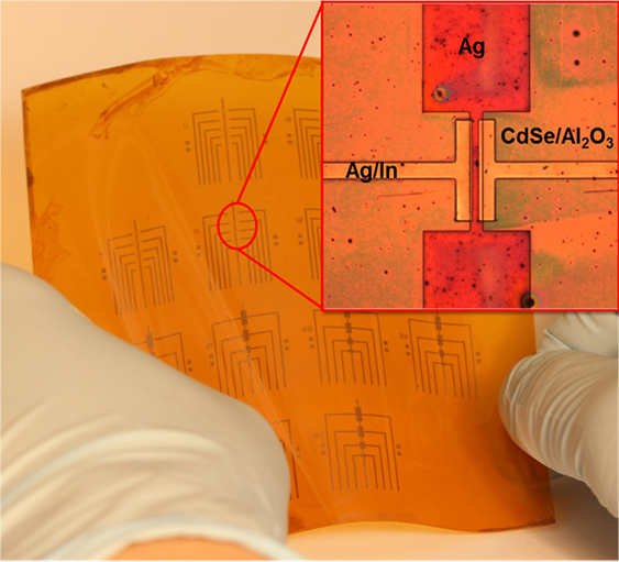
University of Pennsylvania engineers have developed a simplified new approach for making transistors by sequentially depositing their components in the form of liquid nanocrystal “inks.” The new process open the door for transistors and other electronic components to be built into flexible or wearable applications. It also avoids the highly complex current process for creating transistors, which requires high-temperature, high-vacuum equipment. Also, the new lower-temperature process is compatible with a wide array of materials and can be applied to larger areas.
Transistors patterned on plastic backing
The researchers’ nanocrystal-based field effect transistors were patterned onto flexible plastic backings using spin coating, but could eventually be constructed by additive manufacturing systems, like 3D printers.
Published in the journal Science, the study was lead by Cherie Kagan, the Stephen J. Angello Professor in the School of Engineering and Applied Science, and Ji-Hyuk Choi, then a member of her lab, now a senior researcher at the Korea Institute of Geoscience and Mineral Resources. Researchers at Korea University Korea’s Yonsei University were also involved.

Kagan’s group developed four nanocrystal inks that comprise the transistor, then deposited them on a flexible backing. (credit: University of Pennsylvania)
The researchers began by dispersing a specific type of nanocrystals in a liquid, creating nanocrystal inks. They developed a library of four of these inks: a conductor (silver), an insulator (aluminum oxide), a semiconductor (cadmium selenide), and a conductor combined with a dopant (a mixture of silver and indium). (“Doping” the semiconductor layer of a transistor with impurities controls whether the device creates a positive or negative charge.)
“These materials are colloids just like the ink in your inkjet printer,” Kagan said, “but you can get all the characteristics that you want and expect from the analogous bulk materials, such as whether they’re conductors, semiconductors or insulators.” Although the electrical properties of several of these nanocrystal inks had been independently verified, they had never been combined into full devices. “Our question was whether you could lay them down on a surface in such a way that they work together to form functional transistors.”
Laying down patterns in layers
Such a process entails layering or mixing them in precise patterns.
First, the conductive silver nanocrystal ink was deposited from liquid on a flexible plastic surface that was treated with a photolithographic mask, then rapidly spun to draw it out in an even layer. The mask was then removed to leave the silver ink in the shape of the transistor’s gate electrode.
The researchers followed that layer by spin-coating a layer of the aluminum oxide nanocrystal-based insulator, then a layer of the cadmium selenide nanocrystal-based semiconductor and finally another masked layer for the indium/silver mixture, which forms the transistor’s source and drain electrodes. Upon heating at relatively low temperatures, the indium dopant diffused from those electrodes into the semiconductor component.
“The trick with working with solution-based materials is making sure that, when you add the second layer, it doesn’t wash off the first, and so on,” Kagan said. “We had to treat the surfaces of the nanocrystals, both when they’re first in solution and after they’re deposited, to make sure they have the right electrical properties and that they stick together in the configuration we want.”
Because this entirely ink-based fabrication process works at lower temperatures than existing vacuum-based methods, the researchers were able to make several transistors on the same flexible plastic backing at the same time.
The inks’ specialized surface chemistry allowed them to stay in configuration without losing their electrical properties. (credit: University of Pennsylvania)
“Making transistors over larger areas and at lower temperatures have been goals for an emerging class of technologies, when people think of the Internet of things, large area flexible electronics and wearable devices,” Kagan said. “We haven’t developed all of the necessary aspects so they could be printed yet, but because these materials are all solution-based, it demonstrates the promise of this materials class and sets the stage for additive manufacturing.”
Because this entirely ink-based fabrication process works at lower temperatures than existing vacuum-based methods, the researchers were able to make several transistors on the same flexible plastic backing at the same time.
3D-printing transistors for wearables
“This is the first work,” Choi said, “showing that all the components, the metallic, insulating, and semiconducting layers of the transistors, and even the doping of the semiconductor, could be made from nanocrystals.”
“Making transistors over larger areas and at lower temperatures have been goals for an emerging class of technologies, when people think of the Internet of things, large area flexible electronics and wearable devices,” Kagan said. “We haven’t developed all of the necessary aspects so they could be printed yet, but because these materials are all solution-based, it demonstrates the promise of this materials class and sets the stage for additive manufacturing.”
The research was supported by the National Science Foundation, the U.S. Department of Energy, the Office of Naval Research, and the Korea Institute of Geoscience and Mineral Resources funded by the Ministry of Science, ICT, and Future Planning of Korea.
Abstract of Exploiting the colloidal nanocrystal library to construct electronic devices
Synthetic methods produce libraries of colloidal nanocrystals with tunable physical properties by tailoring the nanocrystal size, shape, and composition. Here, we exploit colloidal nanocrystal diversity and design the materials, interfaces, and processes to construct all-nanocrystal electronic devices using solution-based processes. Metallic silver and semiconducting cadmium selenide nanocrystals are deposited to form high-conductivity and high-mobility thin-film electrodes and channel layers of field-effect transistors. Insulating aluminum oxide nanocrystals are assembled layer by layer with polyelectrolytes to form high–dielectric constant gate insulator layers for low-voltage device operation. Metallic indium nanocrystals are codispersed with silver nanocrystals to integrate an indium supply in the deposited electrodes that serves to passivate and dope the cadmium selenide nanocrystal channel layer. We fabricate all-nanocrystal field-effect transistors on flexible plastics with electron mobilities of 21.7 square centimeters per volt-second.
http://www.kurzweilai.net/best-textile-manufacturing-methods-for-creating-human-tissues-with-stem-cells
Elizabeth Loboa, dean of the Missouri University College of Engineering, and her team have tested new tissue- engineering methods (based on textile manufacturing) to find ones that are most cost-effective and can be produced in larger quantities.
Tissue engineering is a process that uses novel biomaterials seeded with stem cells to grow and replace missing tissues. When certain types of materials are used, the “scaffolds” that are created to hold stem cells eventually degrade, leaving natural tissue in its place. The new tissues could help patients suffering from wounds caused by diabetes and circulation disorders, patients in need of cartilage or bone repair, and women who have had mastectomies by replacing their breast tissue. The challenge is creating enough of the material on a scale that clinicians need to treat patients.
Comparing textile manufacturing techniques
 http://www.kurzweilai.net/images/electrospinning.png
Electrospinning experiment: nanofibers are collected into an ethanol bath and removed at predefined time intervals (credit: J. M. Coburn et al./The Johns Hopkins University/PNAS)
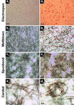
In typical tissue engineering approaches that use fibers as scaffolds, non-woven materials are often bonded together using an electrostatic field. This process, called electrospinning (see Nanoscale scaffolds and stem cells show promise in cartilage repair and Improved artificial blood vessels), creates the scaffolds needed to attach to stem cells.
However, large-scale production with electrospinning is not cost-effective. “Electrospinning produces weak fibers, scaffolds that are not consistent, and pores that are too small,” Loboa said. “The goal of ‘scaling up’ is to produce hundreds of meters of material that look the same, have the same properties, and can be used in clinical settings. So we investigated the processes that create textiles, such as clothing and window furnishings like drapery, to scale up the manufacturing process.”
The group published two papers using three industry-standard, high-throughput manufacturing techniques — meltblowing, spunbonding, and carding — to determine if they would create the materials needed to mimic native tissue.
Meltblowing is a technique during which nonwoven materials are created using a molten polymer to create continuous fibers. Spunbond materials are made much the same way but the fibers are drawn into a web while in a solid state instead of a molten one. Carding involves the separation of fibers through the use of rollers, forming the web needed to hold stem cells in place.
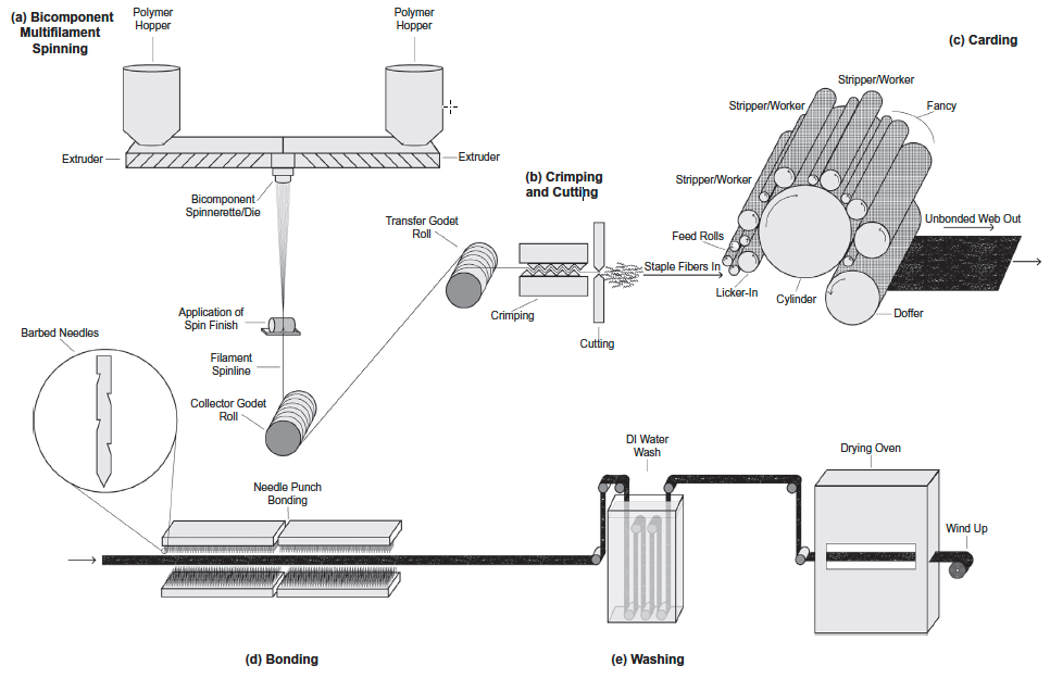
http://www.kurzweilai.net/images/carded-scaffold-fabrication.jpg
Schematic of gilled fiber multifilament spinning and carded scaffold fabrication (credit: Stephen A. Tuin et al./Acta Biomaterialia)
Cost-effective methods
Loboa and her colleagues tested these techniques to create polylactic acid (PLA) scaffolds (a Food and Drug Administration-approved material used as collagen fillers), seeded with human stem cells. They then spent three weeks studying whether the stem cells remained healthy and if they began to differentiate into fat and bone pathways, which is the goal of using stem cells in a clinical setting when new bone and/or new fat tissue is needed at a defect site. Results showed that the three textile manufacturing methods proved as viable if not more so than electrospinning.
“These alternative methods are more cost-effective than electrospinning,” Loboa said. “A small sample of electrospun material could cost between $2 to $5. The cost for the three manufacturing methods is between $.30 to $3.00; these methods proved to be effective and efficient. Next steps include testing how the different scaffolds created in the three methods perform once implanted in animals.”
Researchers at North Carolina State University and the University of North Carolina at Chapel Hill were also involved in the two studies, which were published in Biomedical Materials (open access) and Acta Biomaterialia. The National Science Foundation, the National Institutes of Health, and the Nonwovens Institute provided funding for the studies.
Abstract of Creating tissues from textiles: scalable nonwoven manufacturing techniques for fabrication of tissue engineering scaffolds
Electrospun nonwovens have been used extensively for tissue engineering applications due to their inherent similarities with respect to fibre size and morphology to that of native extracellular matrix (ECM). However, fabrication of large scaffold constructs is time consuming, may require harsh organic solvents, and often results in mechanical properties inferior to the tissue being treated. In order to translate nonwoven based tissue engineering scaffold strategies to clinical use, a high throughput, repeatable, scalable, and economic manufacturing process is needed. We suggest that nonwoven industry standard high throughput manufacturing techniques (meltblowing, spunbond, and carding) can meet this need. In this study, meltblown, spunbond and carded poly(lactic acid) (PLA) nonwovens were evaluated as tissue engineering scaffolds using human adipose derived stem cells (hASC) and compared to electrospun nonwovens. Scaffolds were seeded with hASC and viability, proliferation, and differentiation were evaluated over the course of 3 weeks. We found that nonwovens manufactured via these industry standard, commercially relevant manufacturing techniques were capable of supporting hASC attachment, proliferation, and both adipogenic and osteogenic differentiation of hASC, making them promising candidates for commercialization and translation of nonwoven scaffold based tissue engineering strategies.
Abstract of Fabrication of novel high surface area mushroom gilled fibers and their effects on human adipose derived stem cells under pulsatile fluid flow for tissue engineering applications
The fabrication and characterization of novel high surface area hollow gilled fiber tissue engineering scaffolds via industrially relevant, scalable, repeatable, high speed, and economical nonwoven carding technology is described. Scaffolds were validated as tissue engineering scaffolds using human adipose derived stem cells (hASC) exposed to pulsatile fluid flow (PFF). The effects of fiber morphology on the proliferation and viability of hASC, as well as effects of varied magnitudes of shear stress applied via PFF on the expression of the early osteogenic gene marker runt related transcription factor 2 (RUNX2) were evaluated. Gilled fiber scaffolds led to a significant increase in proliferation of hASC after seven days in static culture, and exhibited fewer dead cells compared to pure PLA round fiber controls. Further, hASC-seeded scaffolds exposed to 3 and 6 dyn/cm2 resulted in significantly increased mRNA expression of RUNX2 after one hour of PFF in the absence of soluble osteogenic induction factors. This is the first study to describe a method for the fabrication of high surface area gilled fibers and scaffolds. The scalable manufacturing process and potential fabrication across multiple nonwoven and woven platforms makes them promising candidates for a variety of applications that require high surface area fibrous materials.
Statement of Significance
We report here for the first time the successful fabrication of novel high surface area gilled fiber scaffolds for tissue engineering applications. Gilled fibers led to a significant increase in proliferation of human adipose derived stem cells after one week in culture, and a greater number of viable cells compared to round fiber controls. Further, in the absence of osteogenic induction factors, gilled fibers led to significantly increased mRNA expression of an early marker for osteogenesis after exposure to pulsatile fluid flow. This is the first study to describe gilled fiber fabrication and their potential for tissue engineering applications. The repeatable, industrially scalable, and versatile fabrication process makes them promising candidates for a variety of scaffold-based tissue engineering applications.
references:
- S A Tuin, B Pourdeyhimi, E G Loboa. Creating tissues from textiles: scalable nonwoven manufacturing techniques for fabrication of tissue engineering scaffolds. Biomedical Materials, 2016; 11 (1): 015017 DOI: 10.1088/1748-6041/11/1/015017 (open access)
- Stephen A. Tuin, Behnam Pourdeyhimi, Elizabeth G. Loboa. Fabrication of novel high surface area mushroom gilled fibers and their effects on human adipose derived stem cells under pulsatile fluid flow for tissue engineering applications. Acta Biomaterialia, 2016; DOI: 10.1016/j.actbio.2016.03.025