Japan’s Ceramics and Glass Industries
Reporter: Aviva Lev-Ari, PhD, RN
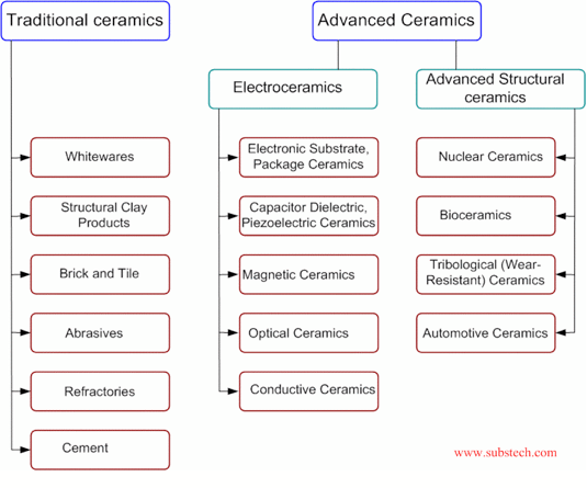
INDUSTRY OVERVIEW
1. Ceramics and Glass Industries in Japan
Applications of structural ceramics in Japan summarized in this review include vacuum process chambers for manufacturing semiconductor and liquid crystal devices, wear-resistant ceramics used for steel-making, optical lens forming and cutting tools, refractory tubes for casting aluminum alloys, and automotive applications.
Ceramic advances in Japan: By Alex Talavera and Randy B. Hecht Achieving new breakthroughs, meeting new challenges
1.1 Applications and New Breakthroughs – Advances in Ceramics and Glass Industries in Japan
Latest Breakthroughs
- Asahi Glass reported that it had developed the world’s thinnest sheet float glass and the world’s thinnest soda-lime glass substrate for touch screens.
- Kyocera unveiled the industry’s first mobile handset “crystal unit” with a precision thermistor.
- Murata became the first manufacturer in the industry to commercialize ceramic capacitors that are designed for automotive uses and certified under the safety standards established to prevent accidents caused by finished products or electronic components.
- The National Institute of Advanced Industrial Science and Technology (AIST) announced that for the first time in the world, it had demonstrated electricity generation by directly reformed fuel at low temperature (450°C).
Ceramic advances in Japan
- Optical technology products, such as 3D optical circuit devices for future optical computers;
- Products for ultrathin plasma televisions, computer screens, reusable cups and bottles;
- Substrates for ultra-high performance DNA analysis chips.
| Company |
Industry |
|
Website : |
| AGC: Asahi Glass |
Automotive; Electronics; Display and Imaging; Life Sciences; Lighting and Optics. |
Lab use ware (beakers and flasks); Glass with high purity for high functionality for semiconductor manufacturing process; Ultra thin slides for microscopes; Glass substrate for display screens of televisions, computers or car navigation systems. |
http://www.agc.com/english/portal/electronics.html |
| Ariake Materials Co. |
Semiconductor and Electric device |
Large size chucking plate for LCD manufacturing process |
http://www.ariake-materials.co.jp/index_e.html |
| Central Glass Co. |
Electronics and Automotive |
Flat Glass for LCD; Semiconductor; |
http://www.cgc-jp.com |
| Ibiden Co. |
Electronics and Automotive |
Ceramic Fiber; Automotive exhaust components, |
http://www.ibiden.com |
| INAX |
Bldg Materials; |
Windows, Bathroom doors, Sanitary wares, Faucets |
http://global.inax.lixil.co.jp/ |
| Kyocera |
Cameras, copiers, printers, mobile phones, electronic and semiconductor components, and optoelectronic products. |
Ceramic capacitors; Ceramic substrates for probe cards, Ceramic for image sensors; Light Emitting Diodes, MEMS Sensors; Timing Devices |
http://global.kyocera.com/ |
| Konoshima Chemical |
Ceramic based building materials and ceramics. |
Nonflammable exterior wall materials; nonflammable interior wall materials for walls in kitchens, toilets, etc.; and fireproofing protection plates and fireproof panels for buildings. And ceramics, such as YAG, TGG, and transparent yttria ceramics. |
http://www.konoshima.co.jp/en/index.html |
| NEG: Nippon Electric Glass |
Electronic Devices; Building materials and Heat resistant glass; Glass Fiber |
Substrate glass for LCD; Glass Tubing for Cold Cathode Fluorescence Lamps; Powder Glass for hermetic seals and insulating films, coating electronic components; Cover Glass for Image Sensors; Glass for Diodes |
http://www.neg.co.jp/EN |
| Murata Manufacturing Company, Ltd. |
Electronic Devices |
Monolithic Ceramic PTC Thermisor |
http://www.murata.com/index.html |
SOURCE
http://www.ceramicindustry.com/articles/print/kyocera-and-japan-medical-materials-open-u-s-design-center
http://journals.cambridge.org/action/displayAbstract?fromPage=online&aid=8188601

SOURCE
http://www.substech.com/dokuwiki/doku.php
Leading Business Players
AGC: Asahi Glass – targets product lines include flat glass; automotive glass; display, electronics and energy devices; and chemicals. Expertise in
- glass
- fluorine chemistry and
- ceramics technologies
- Refractory lining materials for glass melting furnaces that we develop not only tolerate high temperatures but also ensure a high degree of uniformity and composition suited for glass processing, extended the service life of glass melting furnaces
- new materials and products such as semiconductor materials, heat-resistant protective materials and sputtering targets
- thin-glass production technology for displays and info-communication devices, alkalifree glass and measuring just 0.1 mm, the paper-thin sheet float glass was for touch screens and high-tech applications such as medical devices, the substrate is 15 percent lighter and would lend itself to manufacture of smaller, lighter smart phones and tablets.
- AGC glass substrate used in backgrinding processes to reduce the thickness of semiconductor chips
Kyocera, Kyoto
- Its business segments include fine ceramic components, applied ceramic products, semiconductor components, electronic devices, and telecommunications and document imaging equipment. Kyocera has a presence in markets as diverse as solar power generating systems for residential use, medical and dental products, cutting tools, lenses, automotive components, telecommunications equipment and semiconductor equipment.
- Its wafer-processing, lithography,etching, deposition and inspectionsystems have extensive applicationsin semiconductor and LCD processingequipment. Research and developmenton single-crystal-sapphire applications encompass crystal growth for sapphire wafers, plasma etching for sapphire tubes and the fabrication of sapphire windows.
- company unveiled the first cell phone crystal unit package that also contains a thermistor—a temperature sensing component.
- the company announced its selection by Japan’s New Energy and Industrial Technology Development Organization (NEDO) for participation—along with Toshiba, Hitachi, Sharp, NGK Insulators, Itochu Techno-Solutions, NEC and Shimuzu—in a smart-grid demonstration project in New Mexico that will be a collaboration among NEDO, the New Mexico state government, Los Alamos’ Department of Public Utilities and Los Alamos Lab.
- Kyocera also uses alumina and aluminum nitride ceramics to produce multilayer packages and single-layer submounts for high-power, high-brightness LEDs, improving the environment with our components for LED lighting that saves more energy than incandescent lights, has a longer life than fluorescent lighting and uses no toxic substances such as mercury.”
Murata Manufacturing Co.
Murata’s core electronics products have application across diverse industries, including mobile phones, computers, audio-visual equipment, automotive electronics, environment, energy and healthcare. The company’s radiofrequency technology furthers advances in built-in inductors and capacitors for communication applications that allow for the development of more compact communication modules.
- Among their successes are an antilock brake system and electronic stability controls. In 2011, Murata introduced its KCM series of chip monolithic ceramic capacitors. These are equipped with metal pins and designed for automotive electronic devices.
- Murata says it became the first manufacturer to commercialize ceramic capacitors that are designed for these automotive uses and certified under manufacturer to commercialize ceramic safety standards established to prevent accidents caused by finished products or electronic components.
- it is conducting research into nonglass areas such as composite materials and applied thin-film products.
- the company delivered to the Japan Aerospace Exploration Agency ultra-thin lightweight mirrors for use in space-based solar power systems that collect and transmit space harvested solar energy to a receiving facility on Earth. The mirrors were created using NEG’s ultra-thin glass sheet manufacturing and coating technologies.
- the company developed lead-free glass tubes for encapsulating diodes and other chips. NEG says the new glass is also free of halogen-based substances and antimony, and is capable of low-temperature sealing at a level it says is comparable with conventional lead glass.
NEG: Nippon Electric Glass
Nippon Electric Glass develops high tech glass used in flat panel displays, cellular phones, digital cameras and in emerging products within such areas as kitchen appliances, automobiles, and building materials
Research Institutes in Japan
AIST: National Institute of Advanced Industrial Science and Technology
Established as an autonomous entity in 2001, it is the successor to organizations whose work in advanced technology dates to 1882. Its approximately 2,400 researchers.
- mesoporous ceramics research group developed a novel ceramic catalyst capable of killing Escherichia coli and methicillin-resistantStaphylococcus aureus. This ceramic material also is regarded as potentially useful for water decontamination.
- research by the ceramic mechanical parts processing group led to the development of a silicon nitride material that maintains its strength even under large thermal changes. Researchers found that dispersion of fine particles of boron nitride results in dramatic improvement in thermal shock resistance. Published results revealed, “The material does not break and its strength does not decline even when repeatedly dropped into room-temperature water after heating to 1,400°C.
- that research into tough silicon nitride with very high thermal conductivity is among AIST’s most recent achievements
- AIST announced its development of “a technology for direct reforming of a methane-steam fuel at low temperatures by forming a nanometer-scale ceria-based layer as the reforming catalyst on the inner surface of a tubular micro-SOFC with a nickel-based fuel electrode (anode). In addition, for the first time in the world, we have demonstrated the electricity generation by directly reforming the fuel at a low temperature of 450°C.”
Japan Fine Ceramics Center
- “In modern nanotechnology, it is necessary to control atomic structures and electromagnetic properties in nanoscale regions for purposes of creating new materials and devices with a high level of performance,”
- Some examples of its focuses are:
– Electron microscopy and its application to nanotechnology;
– High-efficiency ceramic membranes for high-temperature separation of hydrogen;
– Preparation of specimens of microporous ceramic membranes for highresolution electron microscopy;
– Precise measurement of electric field-induced distortion in piezoceramics; and
– Development of machining techniques for ceramics.
NIMS: National Institute for Materials Science
NIMS is Japan’s only independent administrative institution dedicated to materials science.
- In 2009, NIMS announced successful atomic-level three-dimensional tomography of a stabilized zirconia-spinel nanocomposite.
- This work will trigger applications of the 3DAP technique in nanoscale analyses of a wider variety of inorganic materials.”
- NIMS’ Nano Ceramic Center is dedicated to research into “functional and/ or multifunctional ceramics with novel optical, electric, dielectric, magnetic, thermal, chemical and/or mechanical properties.NIMS are investigating novel techniques of evaluation and design of grain-boundary nanostructures.” NIMS projects include work on- Fabrication of highly structured controlled ceramics through nanoparticle processing in the liquid phase;- Processing for functional ceramics by nanomolecular mixing;- Synthesis of fine nitride particles for optical applications;- Development of multifunctional oxide ceramics by designing grainboundary nanostructures;- Synthesis of functional ceramic nanoparticles through controlled reactive thermal plasma processing; and
- Development of nanostructures through design and modification of nanopores on anodic oxide films.
- Nanotechnology Glass Project says its work can be “classified as belonging to following four fields:- Optical technology products, such as 3D optical circuit devices for future optical computers;- Products for ultrathin plasma televisions, computer screens, reuseable cups and bottles;- Biomedical products to trap endocrine disruption chemicals and separate out harmful gases; and- Substrates for ultra-high performance DNA analysis chips.
SOURCE
http://ceramics.org/wp-content/uploads/2011/10/bulletin-10-11.pdf
1.2 Japan Ceramics & Glass Industry Directory
AGC: Asahi Glass
Www.agc.com/english/index.html
1-5-1, Marunouchi, Chiyoda-ku, Tokyo,
100-8405
Kazuhiko Ishimura, president & CEO
AGC’s English-language “Contact Us” page includes links for email inquiries specific to each of its lines of business:
http://www.agc.com/english/mail_box/
Ariake Materials Co.
http://www.ariake-materials.co.jp/index_e.html
3-3-3 Toyosu, Koto-ku,
Tokyo, 135-6006
Phone: 81-3-5560-2113
Fax: 81-3-5560-2192
Central Glass Co.
http://www.cgc-jp.com/
Denki Kagaku Kogyo KK
http://www.denka.co.jp/eng/top.htm
Shinsuke Yoshitaka, president
FDK Corp.
http://www.fdk.com/
Hamagomu Bldg., 5-36-11
Shimbashi, Minato-ku,
Tokyo, 105-8677
Phone: 81-3-3434-1271
Fax: 81-3-3434-1375
Hitachi
Global Www.hitachi.com/
Ibiden Co.
http://www.ibiden.com
2-1, Kanda-cho, Ogaki,
Gifu 503-8604
Phone: 81-584-81-3111
Ibiden says its primary businesses are electronics- and ceramics-related. Its ceramic products include speciality carbon products and diesel particulate filters.
IHI Aerspace Co.
http://www.ihi.co.jp/ia/en/index.html
Phone: 81-3-6204-7232
Fax: 81-3-6204-8689
INAX
http://global.inax.lixil.co.jp/
INAX is a keystone of LIXIL Corporation, one of Japan’s leading manufacturers of tiling, building materials and sanitary fixtures for residential, commercial and public buildings and facilities. The company says it “looks to create ambience through a distinct vision, texture and form that is based on the company’s origins and historical craft aesthetics.
This essence is not simply a design that suggests or uses Japanese motifs; it is a contemporary expression of a time-honed and honored artisan vision that is borderless, which we call Beaux Japonica.”
Kanto Chemical Co.
http://www.kanto.co.jp/english/
2-1, Nihonbashi Muromachi 2-Chome, Chuo-ku,
Tokyo,103-0022
Phone: 81-3-6214-1050
Fax: 81-3-3241-1007
Konoshima Chemical Co.
http://www.konoshima.co.jp/en/index.html
80 Koda, Takuma-cho, Mitoyo-city,
Kagawa, 769-1103
Phone: 81-875-83-3155
Fax: 81-875-83-8188
Koyo-Sha Co.
http://www.koyo-sha.co.jp/e/index.html
Koyo-Sha Bldg. 9th Floor, No.48-5,
Higashi Nippori 5-Chome, Arakawa-ku,
Tokyo, 116-0014
Phone: 81-3-3805-8375 (International Business Div.)
Fax : 81-3-3805-8369
Krosaki Harima Corp.
http://www.krosaki.co.jp/english/
1-1, Higashihamamachi, Yahatanishiku,
Kitakyushu City, Fukuoka 806-8586
Phone: 81-93-622-7224
Fax: 81-93-622-7200
Kyocera
http://global.kyocera.com/
6 Takeda Tobadono-cho, Fushimi-ku,
Kyoto, 612-8501
Phone: 81-75-604-3416
Fax: 81-75-604-3516
Tetsuo Kuba, president
Mino Yogyo Ceramic Co.
http://www.mino-ceramic.co.jp/english/index.html
Murata Manufacturing Company, Ltd.
http://www.murata.com/index.html
10-1, Higashikotari 1-Chome,
Nagaokakyo-shi,
Kyoto, 617-8555
Phone: 81-75-951-9111
Tsuneo Murata, president
NEG: Nippon Electric Glass
http://www.neg.co.jp/EN/
7-1, Seiran 2-Chome, Otsu,
Shiga, 520-8639
Phone: 81-77-537-1700
Fax: 81-77-534-4967
Masayuki Arioka, president
Nippon Crucible Co.
http://www.rutsubo.com/
1-1, Higashihamamachi, Yahatanishiku,
Kitakyushu City, Fukuoka 806-8586
Phone: 81-3-3443-5551
Fax: 81-3-3443-5191
Nippon Rotary Nozzle Co.
http://www.rotarynozzle.jp/
2-2-1, Otemachi, Chiyodai-ku,
Tokyo 100-0004
NGK Spark Plug
http://www.ngkntk.co.jp/english/index.html
4-18, Takatsuji-cho, Mizuho-ku,
Nagoya, 467-8525
Phone: 81-52-872-5915
Fax: 81-52-872-5999
Shinichi Odo, president and CEO
NGK’s products include sensors, electronic components, industrial components, spark and glow plugs, semiconductor components, medical products and cutting tools. In the latter category, its ceramic grade product(s) are described as “a thermally and chemically stable tool material with a high level of hardness, and it has a compact and fine organization that consists mainly of high-purity alumina.” It is used to cut tube scarfings; for lathe-turning of normal cast iron and materials with a high level of hardness; and for finish-cutting of normal cast iron and ductile cast iron.
Nihon Yamaura Glass Co.
http://www.yamamura.co.jp/english/index.html
Nippon Light Metal Co.
http://www.nlmetal.com/
Tennozu Yusen Bldg., 2-2-20 Higashi-
Shinagawa, Shinagawa-ku,
Tokyo, 140-8628
Phone: 81-3-5461-9211
Nippon Steel
http://www.nsc.co.jp/en/
6-1, Marunouchi 2-Chome, Chiyoda-ku,
Tokyo, 100-8071
Phone: 81-3-6867-4111
Fax: 81-3-6867-5607
Noritake Co.
http://www.noritake-elec.com/
Shinagawa Refractories Co.
http://www.shinagawa.co.jp/English/index.html
2-1 Otemachi 2-chome, Chiyoda-ku,
Tokyo 100-0004
Phone: 81-3-6265-1606
Fax: 81-3-6265-1616
Yoshihiko Shimizu, president
Shoei Chemical Inc.
http://www.shoeichem.co.jp/english/company/index.html
Shinjuku Mitsui Bldg., 1-1 Nishi
Shinjuku 2-Chome, Shinjuku-ku,
Tokyo, 163-0443
Phone: 81-3-3344-6662
Fax: 81-3-3344-6657
Eiichi Asada, president
Shoei Chemical’s work in the development and manufacture of electronic materials focuses chiefly on conductive pastes, resistive pastes, dielective pastes, and powders for use in electronic devices and components. Founded in 1956, the company’s first product was conductive paste made from fine silver powder for use in ceramic disk capacitors. Since then, its new product development has generated more than 100 patents in Japan and abroad. Today, its research efforts are responding to the growing cross-industry demand for electronic components whose sub-micron and nano dimensions deliver miniaturization and higher performance.
Taiko Refractories Co.
http://www.taiko-ref.com/index-e.html
Phone: 81-93-871-1631
Fax: 81-93-883-2151
Hiroshi Kobayashi, president
TDK Corp
http://www.global.tdk.com
1-13-1, Nihonbashi, Chuo-ku, Tokyo
103-8272
Phone: 81-3-3278-5111
TDK says it is basically a ceramics company and a process technology company that uses expertise in ceramics. It notes that it was the first company in the world to commercialize ferrites and that it is a core technology. “TDK’s strength is in using its entire manufacturing capacity to turn the ferrite material into electronic components.”
Toyota Central R&D Labs
http://www.tytlabs.co.jp/eindex.html
41-1, Aza Yokomichi, Oaza Nagakute,
Nagakute-cho, Aichi-gun, Aichi-ken,
480-1192
Shoichiro Toyoda and Masatami Takimoto, CEOs
Established in 1960, Toyota Central R&D Labs Inc. are engaged in basic research in a variety of fields, including resource conservation, energy conservation, environmental preservation and safety so that, in the words of company president Takashi Saito, “we may create a sustainable society.” The enterprise’s research activities fall under four categories: environment, energy, and power train; materials and processing technology; information, safety and comfort, and electronics; and research fundamental technologies.
Toyota Technical Institute
http://www.toyota-ti.ac.jp/english/index-e.htm
2-12-1 Hisakata, Tempaku-ku, Nagoya,
468-8511
Phone: 81-52-802-1111
World Lab Inc.
http://www.tokushinkai.or.jp/english/wl/
3-2-25 Miyuki-cho, Akiha-ku, Niigatacity,
Niigata, 956-0023
Phone: 81-250-23-2009
Fax: 81-250-25-2444
Yageo Corp.
http://www.yageo.com/portal/index.jsp
16th Namiki Building, 3F, 4-116-1,
Miya-cho Omiya-ku, Saitama, 330-0802
Phone: 81-48-795-8953
Fax: 81-48-795-8954
SOURCE
Like this:
Like Loading...