
N3xt generation carbon nanotubes
Larry H. Bernstein, MD, FCAP, Curator
LPBI
Skyscraper-style carbon-nanotube chip design ‘boosts electronic performance by factor of a thousand’

http://www.kurzweilai.net/images/computing-high-rise-architecture.jpg
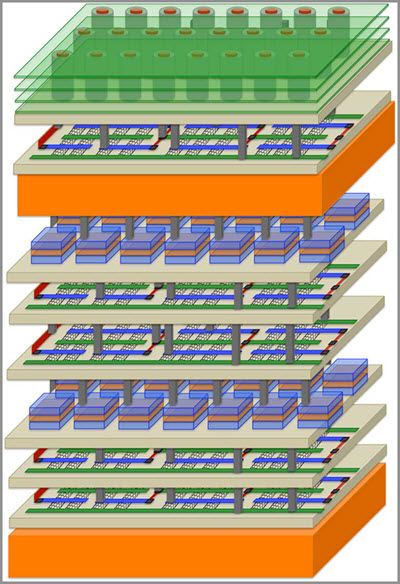
A new revolutionary high-rise architecture for computing (credit: Stanford University)
Researchers at Stanford and three other universities are creating a revolutionary new skyscraper-like high-rise architecture for computing based on carbon nanotube materials instead of silicon.
In Rebooting Computing, a special issue (in press) of the IEEE Computer journal, the team describes its new approach as “Nano-Engineered Computing Systems Technology,” or N3XT.
Suburban-style chip layouts create long commutes and regular traffic jams in electronic circuits, wasting time and energy, they note.
N3XT will break data bottlenecks by integrating processors and memory-like floors in a skyscraper and by connecting these components with millions of “vias,” which play the role of tiny electronic elevators.
The N3XT high-rise approach will move more data, much faster, using far less energy, than would be possible using low-rise circuits, according to the researchers.
Stanford researchers including Associate Professor Subhasish Mitra and Professor H.-S. Philip Wong have “assembled a group of top thinkers and advanced technologies to create a platform that can meet the computing demands of the future,” Mitra says.
“When you combine higher speed with lower energy use, N3XT systems outperform conventional approaches by a factor of a thousand,” Wong claims.
Carbon nanotube transistors
Engineers have previously tried to stack silicon chips but with limited success, the researchers suggest. Fabricating a silicon chip requires temperatures close to 1,800 degrees Fahrenheit, making it extremely challenging to build a silicon chip atop another without damaging the first layer. The current approach to what are called 3-D, or stacked, chips is to construct two silicon chips separately, then stack them and connect them with a few thousand wires.
But conventional 3-D silicon chips are still prone to traffic jams and it takes a lot of energy to push data through what are a relatively few connecting wires.
The N3XT team is taking a radically different approach: building layers of processors and memory directly atop one another, connected by millions of vias that can move more data over shorter distances that traditional wire, using less energy, and immersing computation and memory storage into an electronic super-device.
The key is the use of non-silicon materials that can be fabricated at much lower temperatures than silicon, so that processors can be built on top of memory without the new layer damaging the layer below. As in IBM’s recent chip breakthrough (see “Method to replace silicon with carbon nanotubes developed by IBM Research“), N3XT chips are based on carbon nanotube transistors.
Transistors are fundamental units of a computer processor, the tiny on-off switches that create digital zeroes and ones. CNTs are faster and more energy-efficient than silicon processors, and much thinner. Moreover, in the N3XT architecture, they can be fabricated and placed over and below other layers of memory.
Among the N3XT scholars working at this nexus of computation and memory are Christos Kozyrakis and Eric Pop of Stanford, Jeffrey Bokor and Jan Rabaey of the University of California, Berkeley, Igor Markov of the University of Michigan, and Franz Franchetti and Larry Pileggi of Carnegie Mellon University.
New storage technologies
Team members also envision using data storage technologies that rely on materials other than silicon. This would allow for the new materials to be manufactured on top of CNTs, using low-temperature fabrication processes.
One such data storage technology is called resistive random-access memory, or RRAM (see “‘Memristors’ based on transparent electronics offer technology of the future“). Resistance slows down electrons, creating a zero, while conductivity allows electrons to flow, creating a one. Tiny jolts of electricity switch RRAM memory cells between these two digital states. N3XT team members are also experimenting with a variety of nanoscale magnetic storage materials.
Just as skyscrapers have ventilation systems, N3XT high-rise chip designs incorporate thermal cooling layers. This work, led by Stanford mechanical engineers Kenneth Goodson and Mehdi Asheghi, ensures that the heat rising from the stacked layers of electronics does not degrade overall system performance.
Mitra and Wong have already demonstrated a working prototype of a high-rise chip. At the International Electron Devices Meeting in December 2014 they unveiled a four-layered chip made up of two layers of RRAM memory sandwiched between two layers of CNTs (see “Stanford engineers invent radical ‘high-rise’ 3D chips“).
In their N3XT paper they ran simulations showing how their high-rise approach was a thousand times more efficient in carrying out many important and highly demanding industrial software applications.
references:
- M. Aly, M. Gao, G. Hills, C-S Lee, G. Pitner, M. Shulaker, T. Wu, M. Asheghi, J. Bokor, F. Franchetti, K. Goodson, C. Kozyrakis, I. Markov, K. Olukotun, L. Pileggi, E. Pop, J. Rabaey, C. Ré, H.-S.P. Wong and S. Mitra, Energy-Efficient Abundant-Data Computing: The N3XT 1,000X. IEEE Computer, Special Issue on Rebooting Computing, Dec. 2015 (in press)
This is a little off-thread, but it does involve carbon, so this is the only place I can squeeze this prediction in…
The big news tonight is that the lithium batteries in electric skate boards called “hoverboards” are catching on fire.
This is going to take a lot of them off of the market. But…they will rise again when carbon batteries with graphene and CNTs and boron nitride and I don’t know what else make batteries run as cool as these high-rise CNT chips.
In fact, these high-rise CNT chips will most likely be part of the power control and distribution in the N3XT generation of hoverboards.
I am really curious what will be the next computing paradigm. Personally, I see more than one type of computers being used at the same time : neuromorphic, optical, electronic von Neumann nanotube transistors 3D chips, quantum for some purposes and also magnetic storage (memristors).
What is even more interesting, Mr Kurzweil wrote and said that nanotube high-rise computers like described in the article here will be dominant type of computers in the 20s. It may or may not be true.
Oh for sure, Kynareth, the first von Neumann machines will do their work with these processors. But memristors should also be a part of them.
I suspect that high-rise cnt chips will indeed be dominant as soon as they come to market. This will give you the N3XT “Field of Dreams.”
If you build it they will come. As soon as it is produced in mass quantities, everybody will come and beat down the doors to get them.
This is fantastic. I want the next, or the third next gen of this to be a molecularly built up block of circuitry. This article shows advances using the nano-tube connector that has been experimented before, and also the replacement overall in the circuitry. I only suggest that further generation because it resembles the “molybloc circuits”-bricks and tiles of densely packed circuitry, molybloc standing for molecular block circuitry, found in the Honor Harringoton Sci Fi series (David Weber).
Stanford engineers invent radical ‘high-rise’ 3D chips
http://www.kurzweilai.net/stanford-engineers-invent-radical-high-rise-3d-chips
http://www.kurzweilai.net/images/high-rise-chip.jpg
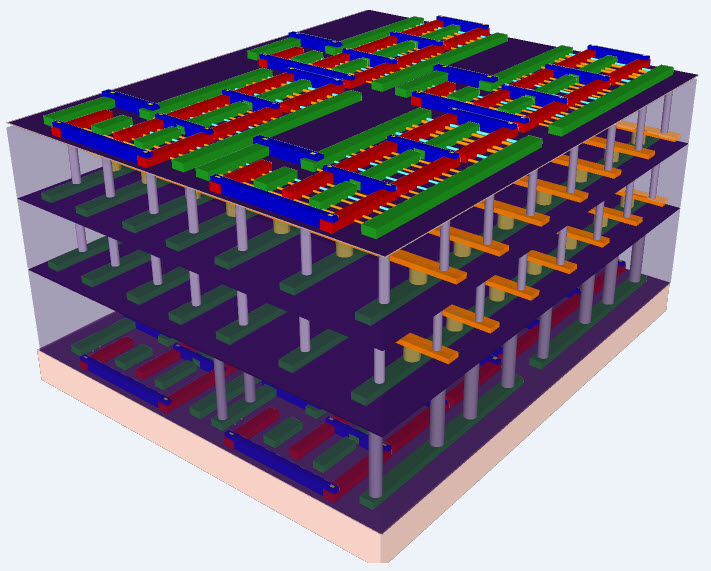
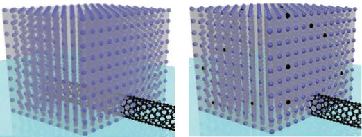
A four-layer prototype high-rise chip built by Stanford engineers. The bottom and top layers are logic transistors. Sandwiched between them are two layers of memory. The vertical tubes are nanoscale electronic “elevators” that connect logic and memory, allowing them to work together efficiently. (Credit: Max Shulaker, Stanford)
Stanford engineers have build 3D “high-rise” chips that could leapfrog the performance of the single-story logic and memory chips on today’s circuit cards, which are subject to frequent traffic jams between logic and memory.
The Stanford approach would attempt to end these jams by building layers of logic atop layers of memory to create a tightly interconnected high-rise chip. Many thousands of nanoscale electronic “elevators” would move data between the layers much faster, using less electricity, than the bottleneck-prone wires connecting single-story logic and memory chips today.
The work is led by Subhasish Mitra, a Stanford associate professor of electrical engineering and of computer science, and H.-S. Philip Wong, the Williard R. and Inez Kerr Bell Professor in Stanford’s School of Engineering. They describe their new high-rise chip architecture in a paper being presented at the IEEE International Electron Devices Meeting Dec. 15–17.
The researchers’ innovation leverages three breakthroughs: a new technology for creating transistors using nanotubes, a new type of computer memory that lends itself to multi-story fabrication, and a technique to build these new logic and memory technologies into high-rise structures in a radically different way than previous efforts to stack chips.
“This research is at an early stage, but our design and fabrication techniques are scalable,” Mitra said. “With further development this architecture could lead to computing performance that is much, much greater than anything available today.” Wong said the prototype chip unveiled at IEDM shows how to put logic and memory together into three-dimensional structures that can be mass-produced.
“Paradigm shift is an overused concept, but here it is appropriate,” Wong said. “With this new architecture, electronics manufacturers could put the power of a supercomputer in your hand.”
Overcoming silicon heat
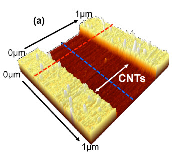
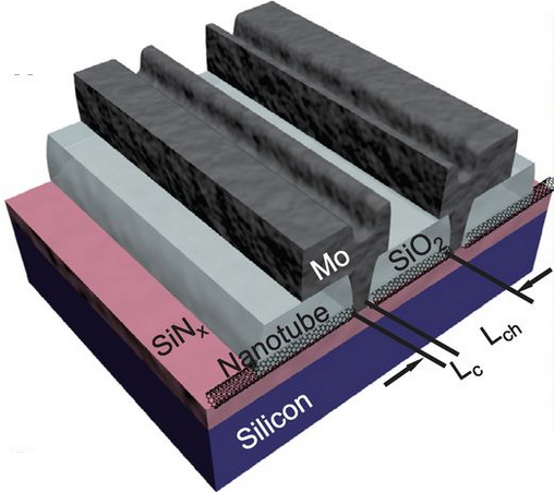
Researchers have been trying to solve a major problem with chip-generated heat by creating carbon nanotubes (CNT) transistors. Mitra and Wong are presenting a second paper at the conference showing how their team made some of the highest performance CNT transistors ever built.

Image of a CNT-based field-effect transistor (FET) using a new high-density process (credit: Mitra/Wong Lab, Stanford)
http://www.kurzweilai.net/images/CNTFET.jpg
Until now the standard process used to grow CNTs did not create sufficient density. The Stanford engineers solved this problem an ingenious technique. They started by growing CNTs the standard way, on round quartz wafers. Then they created a metal film that acts like a tape. Using this adhesive process, they lifted an entire crop of CNTs off the quartz growth medium and placed it onto a silicon wafer that would become the foundation of their high-rise chip.
They repeated this process 13 times, achieving some of the highest density, highest performance CNTs ever made. Moreover, the Stanford team showed that they could perform this technique on more than one layer of logic as they created their high-rise chip.
RRAM memory

Left: Today’s single-story electronic circuit cards, where logic and memory chips exist as separate structures connected by wires, can get jammed with digital traffic between logic and memory. Right: layers of logic and memory create skyscraper chips where data would move up and down on nanoscale “elevators” to avoid traffic jams. (Credit: Mitra/Wong Lab, Stanford)
Wong is a world leader in a new memory technology called “resistive random access memory” (RRAM) which he unveiled at last year’s IEDM conference.
Unlike today’s memory chips, this new storage technology is not based on silicon, but titanium nitride, hafnium oxide and platinum. This formed a metal/oxide/metal sandwich. Applying electricity to this three-metal sandwich one way causes it to resist the flow of electricity. Reversing the polarity causes the structure to conduct electricity again.
The change from resistive to conductive states is how this new memory technology creates digital zeroes and ones.
RRAM uses less energy than current memory, leading to prolonged battery life in mobile devices. Inventing this new memory technology was also the key to creating the high-rise chip because RRAM can be made at much lower temperatures than silicon memory.
Interconnected layers
Max Shulaker and Tony Wu, Stanford graduate students in electrical engineering, created the techniques behind the four-story high-rise chip unveiled at the conference.
The low-heat process for making RRAM and CNTs enabled them to fabricate each layer of memory directly atop each layer of CNT logic. While making each memory layer, they were able to drill thousands of interconnections into the logic layer below. This multiplicity of connections is what enables the high-rise chip to avoid the traffic jams on conventional circuit cards.
There is no way to tightly interconnect layers using today’s conventional silicon-based logic and memory. That’s because it takes so much heat to build a layer of silicon memory — about 1,000 degrees Celsius — that any attempt to do so would melt the logic below.
Previous efforts to stack silicon chips could save space but not avoid the digital traffic jams. That’s because each layer would have to be built separately and connected by wires — which would still be prone to traffic jams, unlike the nanoscale elevators in the Stanford design.
‘Memristors’ based on transparent electronics offer technology of the future

Transparent electronics (pioneered at Oregon State University) may find one of their newest applications as a next-generation replacement for some uses of non-volatile flash memory, a multi-billion dollar technology nearing its limit of small size and information storage capacity.
Researchers at OSU have confirmed that zinc tin oxide, an inexpensive and environmentally benign compound, could provide a new, transparent technology where computer memory is based on resistance, instead of an electron charge.
This resistive random access memory, or RRAM, is referred to by some researchers as a “memristor.” Products using this approach could become even smaller, faster and cheaper than the silicon transistors that have revolutionized modern electronics — and transparent as well.
Transparent electronics offer potential for innovative products that don’t yet exist, like information displayed on an automobile windshield, or surfing the web on the glass top of a coffee table.
“Flash memory has taken us a long way with its very small size and low price,” said John Conley, a professor in the OSU School of Electrical Engineering and Computer Science. “But it’s nearing the end of its potential, and memristors are a leading candidate to continue performance improvements.”
Memristors: faster than flash
Memristors have a simple structure, are able to program and erase information rapidly, and consume little power. They accomplish a function similar to transistor-based flash memory, but with a different approach. Whereas traditional flash memory stores information with an electrical charge, RRAM accomplishes this with electrical resistance. Like flash, it can store information as long as it’s needed.
Flash memory computer chips are ubiquitous in almost all modern electronic products, ranging from cell phones and computers to video games and flat panel televisions.
Thin-film transistors that control liquid crystal displays
Some of the best opportunities for these new amorphous oxide semiconductors are not so much for memory chips, but with thin-film, flat panel displays, researchers say. Private industry has already shown considerable interest in using them for the thin-film transistors that control liquid crystal displays, and one compound approaching commercialization is indium gallium zinc oxide.
But indium and gallium are getting increasingly expensive, and zinc tin oxide — also a transparent compound — appears to offer good performance with lower cost materials. The new research also shows that zinc tin oxide can be used not only for thin-film transistors, but also for memristive memory, Conley said, an important factor in its commercial application.
More work is needed to understand the basic physics and electrical properties of the new compounds, researchers said.
This research was supported by the U.S. Office of Naval Research, the National Science Foundation and the Oregon Nanoscience and Microtechnologies Institute.
Resistive switching in zinc–tin-oxide
Santosh Muralia, Jaana S. Rajachidambaramb, Seung-Yeol Hanb, Chih-Hung Changb, Gregory S. Hermanb, John F. Conley Jr.a,
Bipolar resistive switching is demonstrated in the amorphous oxide semiconductor zinc–tin-oxide (ZTO). A gradual forming process produces improved switching uniformity. Al/ZTO/Pt crossbar devices show switching ratios greater than 103, long retention times, and good endurance. The resistive switching in these devices is consistent with a combined filamentary/interfacial mechanism. Overall, ZTO shows great potential as a low cost material for embedding memristive memory with thin film transistor logic for large area electronics.
Highlights
► We present the first report of resistive switching in zinc–tin-oxide (ZTO). ► ZTO is the leading alternative material to IGZO for TFTs for LCDs. ► ZTO has an advantage over IGZO of lower cost due to the absence of In and Ga. ► Al/ZTO/Pt crossbar RRAM devices show switching ratios greater than 103. ► ZTO shows promise for embedding RRAM with TFT logic for large area electronics.
Memristor; RRAM; Resistive switching; Amorphous oxide semiconductors; Transparent electronics; Zinc–tin-oxide
http://ars.els-cdn.com/content/thumbimage/1-s2.0-S0038110112002304-gr1.sml
Method to replace silicon with carbon nanotubes developed by IBM Research

IBM Research has announced a “major engineering breakthrough” that could lead to carbon nanotubes replacing silicon transistors in future computing technologies.
As transistors shrink in size, electrical resistance increases within the contacts, which impedes performance. So IBM researchers invented a metallurgical process similar to microscopic welding that chemically binds the contact’s metal (molybdenum) atoms to the carbon atoms at the ends of nanotubes.
The new method promises to shrink transistor contacts without reducing performance of carbon-nanotube devices, opening a pathway to dramatically faster, smaller, and more powerful computer chips beyond the capabilities of traditional silicon semiconductors.
“This is the kind of breakthrough that we’re committed to making at IBM Research via our $3 billion investment over 5 years in research and development programs aimed a pushing the limits of chip technology,” said Dario Gil, VP, Science & Technology, IBM Research. “Our aim is to help IBM produce high-performance systems capable of handling the extreme demands of new data analytics and cognitive computing applications.”
The development was reported today in the October 2 issue of the journal Science.
Overcoming contact resistance
![]()
http://www.kurzweilai.net/images/SWNT-transistor-contacts.jpg
Schematic of carbon nanotube transistor contacts. Left: High-resistance side-bonded contact, where the single-wall nanotube (SWNT) (black tube) is partially covered by the metal molybdenum (Mo) (purple dots). Right: low-resistance end-bonded contact, where the SWNT is attached to the molybdenum electrode through carbide bonds, while the carbon atoms (black dots) from the originally covered portion of the SWNT uniformly diffuse out into the Mo electrode (credit: Qing Cao et al./Science)
The new “end-bonded contact scheme” allows carbon-nanotube contacts to be shrunken down to below 10 nanometers without deteriorating performance. IBM says the scheme could overcome contact resistance challenges all the way to the 1.8 nanometer node and replace silicon with carbon nanotubes.
Silicon transistors have been made smaller year after year, but they are approaching a point of physical limitation. With Moore’s Law running out of steam, shrinking the size of the transistor — including the channels and contacts — without compromising performance has been a challenge for researchers for decades.

http://www.kurzweilai.net/images/SWCNT.jpg
Single wall carbon nanotube (credit: IBM)
IBM has previously shown that carbon nanotube transistors can operate as excellent switches at channel dimensions of less than ten nanometers, which is less than half the size of today’s leading silicon technology. Electrons in carbon transistors can move more easily than in silicon-based devices and use less power.
Carbon nanotubes are also flexible and transparent, making them useful for flexible and stretchable electronics or sensors embedded in wearables.
IBM acknowledges that several major manufacturing challenges still stand in the way of commercial devices based on nanotube transistors.
Earlier this summer, IBM unveiled the first 7 nanometer node silicon test chip, pushing the limits of silicon technologies.
END-BONDED CONTACTS FOR CARBON NANOTUBE TRANSISTORS WITH LOW, SIZE-INDEPENDENT RESISTANCE
Science 2 Oct 2015; 350(6256):68–72 http://dx.doi.org:/10.1126/science.aac8006
Moving beyond the limits of silicon transistors requires both a high-performance channel and high-quality electrical contacts. Carbon nanotubes provide high-performance channels below 10 nanometers, but as with silicon, the increase in contact resistance with decreasing size becomes a major performance roadblock. We report a single-walled carbon nanotube (SWNT) transistor technology with an end-bonded contact scheme that leads to size-independent contact resistance to overcome the scaling limits of conventional side-bonded or planar contact schemes. A high-performance SWNT transistor was fabricated with a sub–10-nanometer contact length, showing a device resistance below 36 kilohms and on-current above 15 microampere per tube. The p-type end-bonded contact, formed through the reaction of molybdenum with the SWNT to form carbide, also exhibited no Schottky barrier. This strategy promises high-performance SWNT transistors, enabling future ultimately scaled device technologies.